- 您现在的位置:买卖IC网 > Sheet目录332 > IR21531STRPBF (International Rectifier)IC DRIVER HALF BRIDGE OSC 8SOIC
IR21531(D)(S) & (PbF)
Electrical Characteristics (cont.)
Gate Driver Output Characteristics
Symbol Definition
Min.
Typ.
Max.
Units Test Conditions
V OH
High level output voltage, V BIAS -V O
—
0
100
I O = OA
VOL Low-level output voltage, VO
VOL_UV UV-mode output voltage, VO
—
—
0
0
100
100
mV
I O = OA
I O = OA
V CC ≤ V CCUV -
tr
Output rise time
—
80
150
tf
tsd
td
Output fall time
Shutdown propogation delay
Output deadtime (HO or LO)
—
—
0.35
45
660
0.60
100
—
0.85
nsec
μ sec
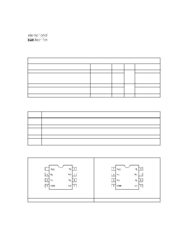
Lead Definitions
Symbol
V CC
R T
C T
COM
LO
V S
HO
V B
Description
Logic and internal gate drive supply voltage
Oscillator timing resistor input
Oscillator timing capacitor input
IC power and signal ground
Low side gate driver output
High voltage floating supply return
High side gate driver output
High side gate driver floating supply
Lead Assignments
8 Lead DIP
IR21531(D)
NOTE: The IR21531D is offered in 8 lead DIP only.
www.irf.com
8 Lead SOIC
IR21531S
5
发布紧急采购,3分钟左右您将得到回复。
相关PDF资料
IR2153DPBF
IC DVR HALF BRDG SELF-OSC 8-DIP
IR2155
IC DRVR HALF BRDG SELF-OSC 8-DIP
IR2181STRPBF
IC DRIVER HIGH/LOW SIDE 8SOIC
IR21834STRPBF
IC DRIVER HALF BRIDGE 14SOIC
IR21844SPBF
IC DRIVER HIGH/LOW SIDE 14SOIC
IR2213SPBF
IC DRIVER HIGH/LOW SIDE 16SOIC
IR22141SSPBF
IC DRIVER HALF BRIDGE SGL 24SSOP
IR2235JPBF
IC DRIVER BRIDGE 3PHASE 44PLCC
相关代理商/技术参数
IR21531STRPBF-CUT TAPE
制造商:IR 功能描述:IR2153 Series 600 V 200 mA 15.6 V Supply Dual Half Bridge Driver - SOIC-8
IR2153D
功能描述:IC HALF BRIDGE DRIVER W/DIO 8DIP RoHS:否 类别:集成电路 (IC) >> PMIC - MOSFET,电桥驱动器 - 外部开关 系列:- 标准包装:50 系列:- 配置:高端 输入类型:非反相 延迟时间:200ns 电流 - 峰:250mA 配置数:1 输出数:1 高端电压 - 最大(自引导启动):600V 电源电压:12 V ~ 20 V 工作温度:-40°C ~ 125°C 安装类型:通孔 封装/外壳:8-DIP(0.300",7.62mm) 供应商设备封装:8-DIP 包装:管件 其它名称:*IR2127
IR2153DPBF
功能描述:功率驱动器IC HALF BRDG DRVR 600V 210mA 1.2us RoHS:否 制造商:Micrel 产品:MOSFET Gate Drivers 类型:Low Cost High or Low Side MOSFET Driver 上升时间: 下降时间: 电源电压-最大:30 V 电源电压-最小:2.75 V 电源电流: 最大功率耗散: 最大工作温度:+ 85 C 安装风格:SMD/SMT 封装 / 箱体:SOIC-8 封装:Tube
IR2153DS
制造商:未知厂家 制造商全称:未知厂家 功能描述:Half Bridge Driver. LO In Phase with RT. Programmable Oscillating Frequency. 1.2us Deadtime in a 8-lead SOIC package with bootstrap diode
IR2153PBF
功能描述:功率驱动器IC HALF BRDG DRVR 600V 15.6Vclamp 1.2 RoHS:否 制造商:Micrel 产品:MOSFET Gate Drivers 类型:Low Cost High or Low Side MOSFET Driver 上升时间: 下降时间: 电源电压-最大:30 V 电源电压-最小:2.75 V 电源电流: 最大功率耗散: 最大工作温度:+ 85 C 安装风格:SMD/SMT 封装 / 箱体:SOIC-8 封装:Tube
IR2153S
功能描述:IC DRVR HALF BRDG SELF-OSC 8SOIC RoHS:否 类别:集成电路 (IC) >> PMIC - MOSFET,电桥驱动器 - 外部开关 系列:- 标准包装:50 系列:- 配置:低端 输入类型:非反相 延迟时间:40ns 电流 - 峰:9A 配置数:1 输出数:1 高端电压 - 最大(自引导启动):- 电源电压:4.5 V ~ 35 V 工作温度:-40°C ~ 125°C 安装类型:表面贴装 封装/外壳:TO-263-6,D²Pak(5 引线+接片),TO-263BA 供应商设备封装:TO-263 包装:管件
IR2153SPBF
功能描述:功率驱动器IC HALF BRDG DRVR 600V 15.6Vclamp 1.2 RoHS:否 制造商:Micrel 产品:MOSFET Gate Drivers 类型:Low Cost High or Low Side MOSFET Driver 上升时间: 下降时间: 电源电压-最大:30 V 电源电压-最小:2.75 V 电源电流: 最大功率耗散: 最大工作温度:+ 85 C 安装风格:SMD/SMT 封装 / 箱体:SOIC-8 封装:Tube
IR2153STR
功能描述:IC DRVR HALF BRDG SELF-OSC 8SOIC RoHS:否 类别:集成电路 (IC) >> PMIC - MOSFET,电桥驱动器 - 外部开关 系列:- 标准包装:50 系列:- 配置:低端 输入类型:非反相 延迟时间:40ns 电流 - 峰:9A 配置数:1 输出数:1 高端电压 - 最大(自引导启动):- 电源电压:4.5 V ~ 35 V 工作温度:-40°C ~ 125°C 安装类型:表面贴装 封装/外壳:TO-263-6,D²Pak(5 引线+接片),TO-263BA 供应商设备封装:TO-263 包装:管件
